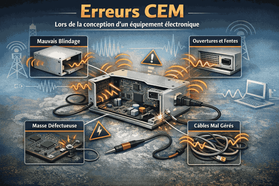
In electronics, pressure on schedules, costs and time to market pushes design teams to deal with function and performance first. Electromagnetic compatibility is then treated as a final validation step rather than as a design parameter in its own right; our article on what EMC is covers the basics. Nemko, a test laboratory, lists this among the ten most common causes of failed EMC tests and calls it perhaps the most common and the most avoidable.
⏳ Why EMC is often dealt with too late
In many projects, EMC is only looked at once a first working prototype exists, or after a first visit to the test laboratory. The reasons are familiar:
- the wish to keep early costs down;
- electromagnetic effects that are underestimated;
- the idea that corrections can always be made later.
According to a study by Intertek, only about half of products pass their EMC tests first time. When the formal test is the first time EMC is evaluated, a failure can mean a redesigned circuit board, changed components, extra prototypes, several rounds of testing and a schedule that slips.
⚠️ The most common EMC mistakes at the design stage
1. Neglecting shielding continuity
A metal enclosure is often taken for a sufficient shield. But it is made of several parts, and covers, hatches and screwed interfaces all create seams. Without good electrical contact along each of them, the enclosure performs well below what its metal would allow.
2. Underestimating openings
The openings needed for cooling, connectors and displays are weak points. A slot about half a wavelength long radiates very efficiently, so a ventilation slot that looks harmless on the drawing can behave like an antenna at some frequencies. For a given open area, many small holes are much better than a few large ones.
3. Poor grounding
Signal currents always return to their source, by the path of least impedance. If that path was not designed, the current finds one anyway, and the larger the loop it follows, the more it radiates. Two ideas are frequently confused here: ground is a zero-volt reference, not a current return path. Metal parts of significant size that are left unbonded to that reference can become the other half of an unintentional antenna.
4. Treating cables and harnesses as secondary
Cables tend to enter the EMC discussion late, although they are one of the most common sources of EMC problems: a cable attached to a board can act as a relatively efficient antenna. A single unshielded, unfiltered wire passing through the wall can cancel the benefit of a shielded enclosure, and a cable shield is effective only if it makes metal-to-metal contact with the enclosure all round the connector.
5. Mechanical interfaces designed without EMC in mind
Assembly clearances, tolerances and finishes are ordinary mechanical decisions, and each one affects contact. An anodised or painted face does not conduct; two surfaces that look flat still leave gaps between them. Even small changes to an enclosure can have a measurable effect on EMC results.
🔧 What a late fix usually looks like
After a first failed test, these faults are corrected with parts added to the existing design:
- conductive EMC gaskets along a seam;
- fabric-covered foam gaskets where the cover cannot press hard;
- contact fingers or another grounding contact on a door or a panel;
- local RF shielding over the circuit that radiates.
These parts help. Fitted late, they often force mechanical changes: a groove to machine, a cover to stiffen, a finish to remove from a contact face.
📐 Building EMC in from the start
The same parts can be planned from the first drawing:
- space reserved for a gasket, with a groove or a compression stop;
- contact faces kept free of paint and anodising;
- a grounding scheme decided before the layout, not after;
- external connectors grouped on the same edge of the board, and cable entries chosen with the shield in mind.
Pre-compliance tests during development show whether these choices work while changes are still manageable.
📘 EMC and compliance testing
EMC tests check that a product stays within the emission limits and reaches the immunity levels set by the standards. Many failures stem from the same underlying design issues, the ones listed above, rather than from a setting that needs adjusting.
✅ In short
EMC is not a constraint to deal with at the end of a project. Seams, openings, grounding, cables and mechanical interfaces are decided early, and so is the EMC behaviour of the equipment. Planning them from the start avoids late corrections and leaves room for the parts that keep an enclosure continuous.
❓ Frequently asked questions
What is EMI and EMC in PCB design?
EMI, electromagnetic interference, is the disturbance; EMC, electromagnetic compatibility, is the aim. On a circuit board it comes down to a few rules: keep the loops followed by high-frequency currents small, do not split or cut the signal return plane, do not place fast circuits between two connectors, and do not make signal edges faster than the function needs.
How do you stop EMI interference?
It is reduced rather than stopped, in two ways. Avoidance acts on the source: remove it or lower its emissions. Mitigation acts on the path: filtering on the cables, shielding around the circuit or the enclosure. Both are easier to apply during design than after a failed test.